PD1500A Double-Pulse Test DUT Parameter Fields
Many DUT Test parameters can be obtained from the DUT device data sheet.
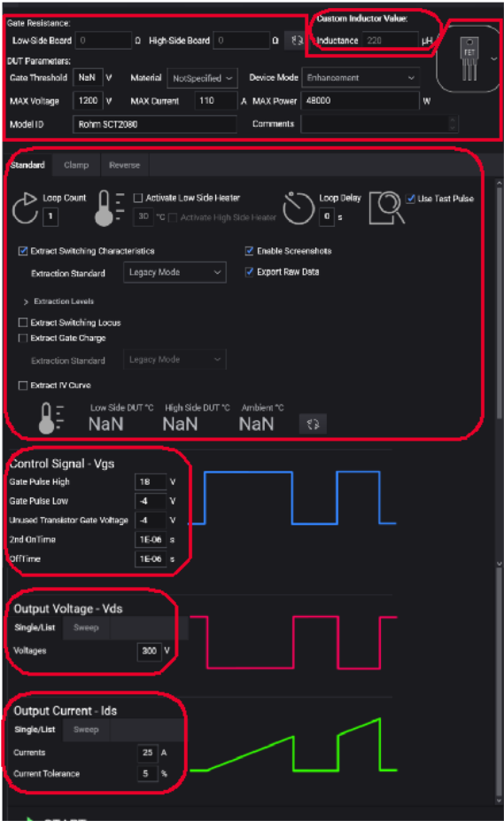
Gate Resistance
For Si/SiC Test Modules
All of the Keysight Si/SiC Gate Drive Modules have two series resistors for the Gate Resistor. Both resistors are the same value. For example, the PD1000-66544
10 W Gate Drive Module has two 4.99 W resistors in series for the 9.98 W RG. The Control Software reads the value of one of the two Gate resistors from the Low-Side Gate Drive module and displays the value here. For the Low-Side gate resistance, the actual measured/calibrated value is displayed; for the High-Side gate resistance, only the nominal value is displayed.
Remember, both the High-Side and Low-Side Gate Drive modules should have gate resistors, RG, of the same resistance.
For Gate Drive modules with no installed gate resistor (the PD1000-66540 and -66541 modules), RG is measured during system calibration which must be done prior to running Double-Pulse tests.
For GaN Test Boards
Refer to the user guide for the specific GaN Test Board that you have. contact your Keysight Application Engineer.
Click the refresh button next to the Gate Resistance to force the software to read the current gate resistor value. Do this when you first start the Control Software and anytime you change the Gate Drive Modules. This also ensures the resistor has not failed.
 Top
TopCustom Inductor Value
Inductance: With software version 2020.820 (and later) you have the option to use the standard, internal inductor (internal to the PD1500A Test Fixture) or an external, custom inductor. Custom Inductor Value appears only if you have specified using a custom inductor in the Hardware Configuration > Inductor Settings dialog. See Step 2: Double-Pulse Test Hardware Configuration
If you are using an external inductor, enter the value of the inductor in the Hardware Setting screen . The value appears in the Custom Inductor Value > Inductance field.
Refer to the PD1500A Using an External Inductor (PD1500-90006) for detailed information about selecting (or designing your own) and installing an external inductor on the PD1500A Test Fixture DUT module.
DUT Parameters
Device Type (Drop-down menu item):
Select either FET, IGBT, or GaN for the Device Under Tested (DUT).
IMPORTANT: Testing GaN devices require a special DUT Test Board and a license for the control software. Contact your local Keysight Application Engineer for availability and information.
Gate Threshold:
Enter the Gate Threshold voltage from the device data sheet. If it is not available, enter “NaN” {(not a Number).
Material (Drop-down menu item):
Select either Si for Silicon or SiC for Silicon Carbide. This is generally available from the device data sheet. If unknown, select Not Specified.
Device Mode:
(not available for IGBT device type) Select either Enhancement Mode (normally off device) or Depletion Mode (normally on device) for GaN or regular FETs. Refer to device data sheet. Default is Enhancement Mode.
MAX Voltage:
Specify the maximum voltage (VDSS or VCES) that may be applied across the device (Drain to Source or Collector to Emitter). Obtain value from the device data sheet.
MAX Current:
Specify the maximum current (ID or IC) that may be used to test the DUT (Drain to Source or Collector to Emitter). Obtain value from the device data sheet.
MAX Power:
Specify the maximum power that may be applied to the DUT. This value is generally not specified on the device data sheet.
As a general guideline, the typical operating voltage for a FET or IGBT is much lower than the Maximum Rated voltage (VDSS or VCES). The following examples are typical and not hard rules:
VDSS Rating: Typical Operating Voltage:
600 V 400 V
1200 V 600 V
1700 V 900 V
Model ID:
A text field to enter the model or device type of the DUT, or any other text information you want to record. Characters not legal for file paths (e.g., \, /, ?, <, >, ...) are replaced by the character “_”. If nothing is entered, the word “Unknown” is used.
Comments:
Allows you to enter comments such as test details or DUT details. Comments are saved as part of the Measurement History and in the Parameters Results page.
Tests - Standard, Clamp, Reverse
Loop Count:
Specify the number of times to repeat the DPT test with the current parameter settings.
Looping or Sweeping Multiple DPT Tests.
Looping or Sweeping Multiple DPT Tests. When running multiple tests on a device, loops are nested:
Loop Count {
Temperature {
Sweep Voltage Values (VDS) {
Sweep Current Values (IDS)
}
}
}
That is, all “Sweep Current Values” are tested before incrementing the “Sweep Voltage Value”. All “Sweep Voltage Values” are tested before incrementing “Temperature”. All “Temperatures” are tested before incrementing “Loop Count”. When looping DPT tests, all measurement data is saved in the directory specified in the Settings > Global Settings menu.
Activate Low Side Heater:
Turns the heater circuit on or off. Remember to set the Temperature Control Settings in the Hardware Configuration > Fixture menu (see “Temperature Control Settings). See Appendix B for a detailed description about using device heaters with the Double-Pulse Test Control Software.
Temperatures:
Enter a single value or a semicolon (;) delimited list of temperatures to heat the device to when running the DPT tests. 175 °C Maximum. This box is grayed-out unless Activate Low Side Heater is checked. See Note, “Looping or Sweeping Multiple DPT Tests”.
Loop delay:
Specify the delay time (in seconds) for the DPT test to idle before running each DPT test in a loop. This time allows the device to cool if you use the heater.
Looping or Sweeping Multiple DPT Tests. When running multiple tests on a device, loops are nested:
Loop Count {
Temperature {
Sweep Voltage Values (VDS) {
Sweep Current Values (IDS)
}
}
}
That is, all “Sweep Current Values” are tested before incrementing the “Sweep Voltage Value”. All “Sweep Voltage Values” are tested before incrementing “Temperature”. All “Temperatures” are tested before incrementing “Loop Count”. When looping DPT tests, all measurement data is saved in the directory specified in the Settings > Global Settings menu.
Use Test Pulse (check box):
When checked, click Start to run a low voltage/low current Double-Pulse Test (50 VDS) before the actual measurement begins. This verifies that the DUT is functional and has not been destroyed. Note, because of the low voltage/low current, the IG and IDS measurements will appear noisy on the oscilloscope. If the Test Pulse measurement succeeds, the complete test runs at full voltage and current. The Test Pulse is available only in Standard Test mode, not for Clamp and Reverse measurements.
Extract Switching Characteristics (check box):
If not checked, only the Extract Gate Charge, Enable Screenshots, and Export Raw Data check boxes are available. When it is checked, an Extraction Standard drop-down menu, the Extract Switching Locus and Extract IV Curve check-boxes become available.
Extraction Standard:
Select Legacy Mode, IEC 60747-8 for FETs, or IEC 60747-9 for IGBTs.
- In Legacy mode, 0 V is defined as 0% for both enhancement mode and depletion mode FETs; The measured VDS is used as 100%.
- In the IEC modes, 0 V is 0% for enhancement mode FETsbut the negative VGS start voltage is used for depletion mode FETs; the set VDS value is used as 100%.
Extraction Levels:
This allows you to specify exact voltage levels for data extraction.
Use Gate Pulse Low for 0% of Vgs:
For Enhancement Mode (normally off devices), use either 0 V or the specified negative Gate Pulse low voltage is used. For Depletion Mode devices, the specified negative Gate Pulse Low voltage is always used.
Extract Switching Locus:
This allows you to specify the percentage used for ID/IC Turn Off level. Switching locus represents the voltage and current combination (ID / VDS) along turn-on and turn-off. It is generally used to make sure the locus is within the Safe Operating Area (SOA) of a device. Switching locus does not follow a standard. It shows output current over output voltage during the switching periods. The switching locus can be generated for any power transistor and the algorithm is independent from semiconductor material or device topology.
For turn-off:
- Starts when the output voltage starts changing
- Stops when output current stops changing
For turn-on:
- Starts when the output current starts changing
- Stops when output voltage stops changing
The switching locus for turn-on and turn-off starts and stops at 0, unless there are no measured values close to 0. In this case, warnings are written to the log file.
For more information, see Parameter Extraction Techniques.
Extract Gate Charge:
(available only in Standard DPT Test) Gate charge characteristics are generally defined by JEDEC and is used to measure the input charge of gate-controlled power transistors. These include FETs and IGBTs. There is also a standard by IEC. Extracts and plots Gate Charge information. Allows you to specify either the Legacy mode or the JESD 24-2 definitions for Gate Charge. Accurate Gate Charge measurements require a high gate resistor (RG) value; typically 100 W or greater. Refer to the PD1000A online help file for details.
Extract IV Curve (checkbox, available only in Standard DPT Test):
This checkbox is grayed-out (not available) unless the Extract Characteristics box is checked. If checked, the complete I/V derivation is extracted and saved. If a Gate Drive Module with a gate resistor (RG) 10 W or greater was used in the DPT test, then the Gate Charge data is displayed. Note: 100 W Gate Resistor (RG) or larger is recommended for IV derivation.
Vgs Resolution:
This field is grayed-out (not available) unless the Extract IV Curve box is checked. Enter a single value to be is used for the extraction of the IV curves.
Enable Screenshots:
Allows user to enable/disable the system automatically taking oscilloscope screen captures during a DPT test. Screen captures are stored in the test subfolder.
- When disabled (default setting), the only screen captures taken are the Summary.png and the PulseAdjustment.png.
- Disabling can shorten the Standard DPT test time.
- Enabling screen captures allows for easier test debugging.
Export Raw Data:
When checked, it enables the export of raw curve data from the oscilloscope. When unchecked, the “Oscilloscope Capture” is not displayed or saved and can decrease the Double-Pule Test Time.
Clamp Voltage:
(available only in Clamp DPT Test). Clamp voltage is fixed at 8 VDC and cannot be changed.
Extract RDS(ON):
(available only in Clamp DPT Test) RDS(ON) stands for “Drain-Source On Resistance. This is the total resistance between drain and source when the FET is “on”. It is the basis for the maximum device current rating. See Static and Dynamic RDS,ON.
Additional Dynamic Extraction:
(available only in Clamp DPT Test). TM,ON is used for the dynamic RDS,ON measurement. This means that it RDS,ON is measured in the 2nd pulse. It should be specified as a value which is larger than zero (0) and smaller than 2nd on-time and is measured from the beginning of the 2nd on-time pulse.
Unless you specify a tm,on time under Additional Dynamic Extraction, only one pulse is used for the RDS,ON Clamp test.
Expected Irrm:
(available only in Reverse DPT Test). Maximum Reverse Recovery Current of a fast or ultrafast diode; such as often used in switch-mode power supplies). Enter the maximum current the body diode is rated for.
- Current Smoothing Number: (available only in Reverse DPT Test). The output current signal is smoothed before extraction. IRRM is extracted with this smoothed signal. For each other extraction (tRR, charge, with this smoothed signal. For each other extraction (tRR, charge, energy, di/dt, ti) an additional user smoothing (default of 10 smoothing points) is applied.
- Integration End Time Threshold: (available only in Reverse DPT Test). The software searches for first crossings of 0.0 A, and first crossing of 0.25 IRM after current peak, etc. Default is 0.25 (25%); range is 0% to 99%. If you select "Enable Screenshots" for the extraction, you can see the measured time of Irrm*25% in the RevRec_trr.png and RevRec_trr_zoomed.png images.
Low-Side DUT °C:
Indicates the temperature of the DUT if the Heater/Thermocouple assembly is connected to the Test Fixture. If the Heater/Thermocouple assembly is not connected to the test fixture or if Activate Heater is not selected, NaN (Not a Number) is shown.
High-Side DUT °C:
Not used in this version of software. Reserved for future use.
Ambient °C:
Indicated the ambient temperature inside the Safety Hood enclosure. Sources for the temperature readings are three internal fixture sensors.
Click the Refresh button to read the current temperatures. See Using the Optional Device (DUT) Heater and Thermocouple for a detailed description about using the device heater with the Double-Pulse Test Control Software.
Measurement Parameters for Standard, Clamp, and Reverse Tests
Control Signal (Gate Voltage (VGS or VGE)):
Gate Pulse High:
A single voltage level of the turn-on Gate Pulse. For the Standard and Clamp tests, this is for the Low-Side device (DUT). For the Reverse Recovery test, this is for the High-Side device. Minimum value for the Gate Pulse High = +13 V. Maximum value = +29 V. The difference between Gate Pulse High and Gate Pulse Low must be less than 30 V.
Gate Pulse Low:
The voltage level of the Gate Pulse; used to ensure the DUT is fully turned off. For the Standard and Clamp tests, this is for the Low-Side device (DUT). For the Reverse Recovery test, this is for the High-Side device. Minimum value = -10 V. Maximum value = 0 V.
The maximum difference between Gate Pulse High and Gate Pulse Low must not exceed 30 V.
Unused Transistor Gate Voltage:
This sets the Gate Voltage for the device not being tested. For the Standard and Clamp tests, this is the High-Side device (DUT). For the Reverse Recovery test, this is the Low-Side device.
2nd On Time:
Enter the time, in microseconds, when the DUT is turned on a second time (and VDS is minimum). For example, 2 microseconds is expressed as “2E-6”. Minimum 200 nS, Maximum 10 mS.
Off Time:
Enter the time, in microseconds, between when the DUT is turned off (and VDS is maximum) and when the DUT is turned on a second time. For example, 2 microseconds is expressed as “2E-6”. Minimum 200 nS, Maximum 25 mS.
Keep 2nd On Time and Off Time as short as possible. IGBT and some other slow devices may require longer times. The pulse width must be long enough that the transistor turns fully on (e.g., > 1 mS). However, the pulse width must not be too long, otherwise, the measurement will be influenced by self-heating of the transistor. 200 nS is the minimum time.
Enter the time, in microseconds, when the DUT is turned on a second time (and VDS is minimum). For example, 2 microseconds is expressed as “2E-6”.

Output Voltage (VDS or VCE):
The Double-Pulse Test can either test at a single VDS/VCE Output Voltage, a list of semicolon-separated Output Voltages, or sweep a series with multiple VDS/VCE Output Voltages.
GaN devices have different system limits than FET or IGBT devices. GaN devices are limited to:
Maximum System Voltage ¡ 500 V
Minimum System Current: ¡ 1 A
Maximum System Current ¡ 100 A
The maximum test voltage that may be applied to the Clamp Circuit Module is 400 V. This for both IGBT and FET devices.
For the Clamp DPT test, use the Clamp Circuit Module and do not install the N2819A Differential Probe. Instead, install one N2873A 10:1 Oscilloscope Probe that connects to the Clamp Test Module (VCLAMP) probe socket. Do not exceed 400 Volts VDS or VCE.
Single/List or Sweep tabs:
If Single/List tab is selected, then run test with a single voltage or a semicolon (;) delimited list of voltages (e.g., 20; 50; 100; 200; ...).
If Sweep is selected, then enter the starting voltage, the ending voltage, and the number of points (voltages) to test. See Sweeping Voltage Example below.
- Minimum Voltage = 50 V, Maximum Voltage = 1200 VDC. Note: Beginning with PD1000A Control Software version 2022.321 (or later), the minimum VDS voltage was reduced to 1 V. On previous SW versions, minimum VDS was 50 V.
# of Points:
Sets the number of voltages between Start and Stop for sweeping.
As a sweep example, suppose you want to run Double-Pulse Tests at the following VDS/VCE voltages: 100, 150, 200, 250, 300, 350, 400 Volts.
- Check the Sweep tab.
- Set Start to: 100.
- Set the Stop to: 400,
- Set the # of Points to: 7. This sets the Step Size to 50 V.
- Then click Start to run the test.
Output Current (IDS or ICE):
The Double-Pulse Test can either test at a single IDS or ICE Output Current, a semicolon-separated list, or sweep with multiple IDS or ICE Output Currents.
Single/List or Sweep tabs:
If Single/List tab is selected, then run test with a single current or a semicolon (;) delimited list of currents (e.g., 20; 35; 50; ...).
If Sweep is selected, then enter the starting current, the ending current, and the number of points (currents) to test. See note below: Sweeping Current Example.
- Minimum current = 10 A, Maximum current = 200 A.Single/List or Sweep tabs: If Single/List tab is selected, then run test with a single current or a semicolon (;) delimited list of currents (e.g., 20; 35; 50; ...).
# of Points:
Sets the number of current values between Start and Stop for sweeping.
As a sweep example, suppose you want to run Double-Pulse Tests at the following IDS or ICE currents: 10, 15, 20, 25, 30, 35, 40 Amps.
- Check the Sweep tab.
- Set Start current to 10.
- Set the Stop current to 40,
- Set the # of Points to 7. This sets the Step Current to 5.00 A.
- Then click Start to run the test.
Current Tolerance %:
Specify a Tolerance value used is setting the pulse width to obtain current values. For example, if you specify a current of 40 A and a tolerance of 5% then the actual current used in the test will be between 38 and 42 A. Value must be greater than zero (0).
Run the Characterization Test
After selecting the type of test (Standard, Clamp, or Reverse Recovery) setting the test parameters::
- Click the Start button to start a measurement or a loop of measurements.
- Stop an active measurement by clicking the Stop button.
- The DPT Control Software calculates the amount of energy that it needs to store in the inductor for the complete test and sets the width of the first pulse accordingly.
- Watch the Progress details just above the Start button.
- After the test runs, and if Enable Screenshots is checked, the Oscilloscope Capture plot and other test data appear in the software display (right side of the display) on the host PC. See Measurement Results Screens.
Test result data is automatically stored in the file specified in the Global Settings > Output Directory (see Double-Pulse Test Output File Structure).